Introduction.
The AWB aligner-bonder provides for complete bonding process control within a single chamber and is ideally-suited to R&D and high-yield production.
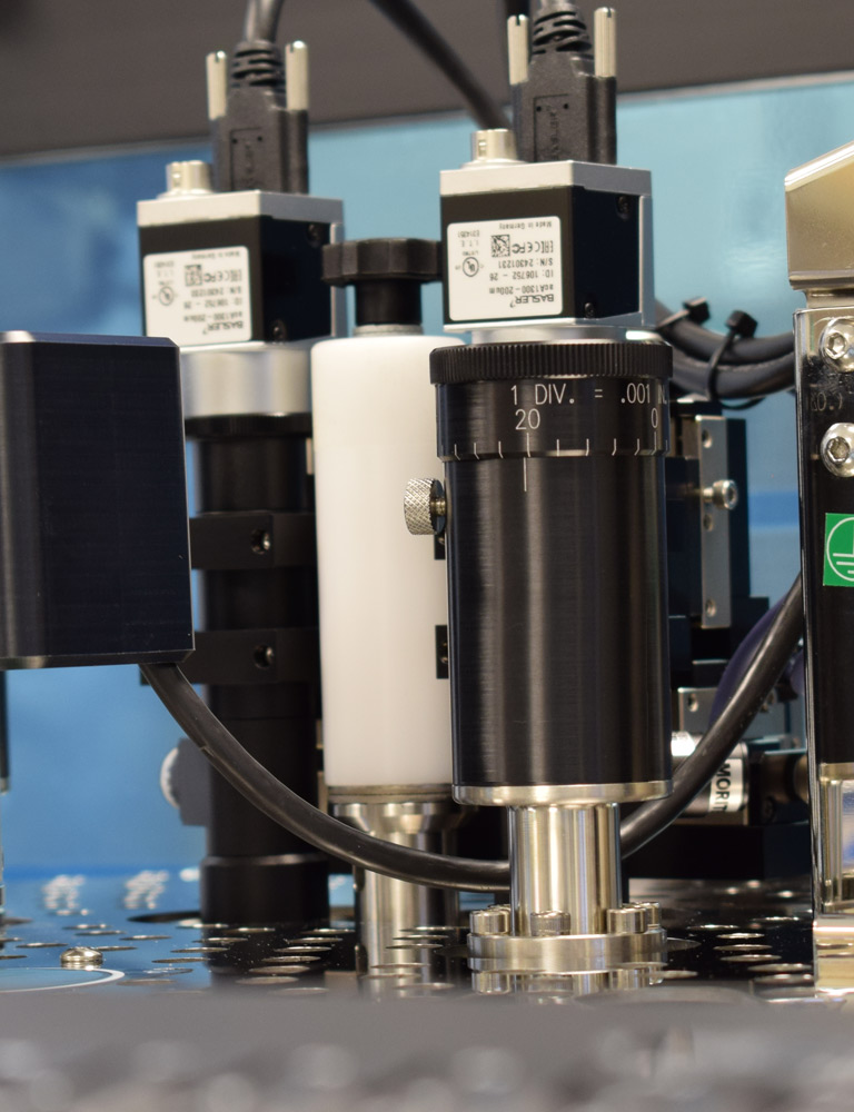
The Bonder provides outstanding flexibility and offers the capabilities for a wide range of bonding techniques. It features a unique in-situ, optical wafer-to-wafer alignment system as standard, with 1μm alignment accuracy.
Configurations.
FOR 3", 4" & 6" WAFERS + CUSTOM CHIPS
AWB 04
FOR 6" & 8" WAFERS
AWB 08
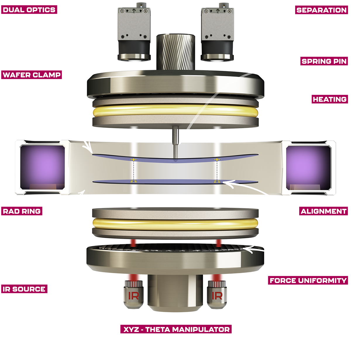
System schematic.
The diagram below is a representation of the components within the AWB chamber.
Key features of the AWB.
In-situ alignment, independent wafer heating and radical activation are amongst many valuable features offered by the system.
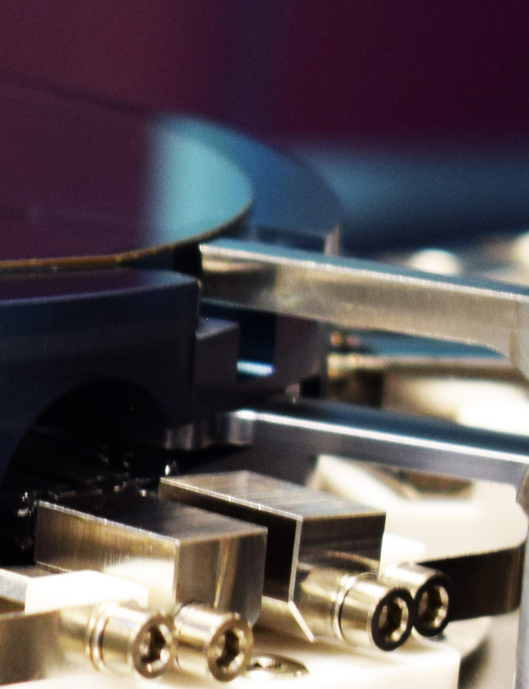
Edge Clamping ensures no contact with bonding surfaces and eliminates the risk of contamination or damage.
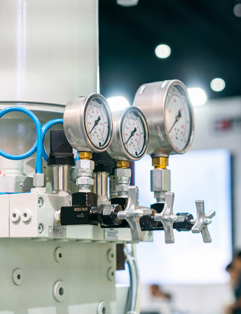
Bonding under vacuum or controlled pressure in the range 2.5 x 10⁻³ mbar and 2 bar absolute. Up to three process gas lines are available.

Motorised Z control to apply contact forces of up to 40kN.
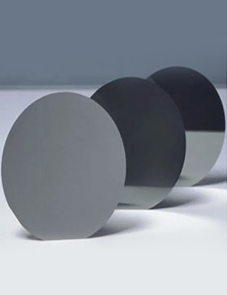
Triple-stack anodic bonding of both combinations: silicon-glass-silicon and glass-silicon-glass is possible.

Optional components for UV cure adhesive bonding are available.

Optional NIR cameras sensitive beyond 1.1μm wavelength can replace the standard cameras if required.

A special upper platen for mounting of a chip can be offered. Custom size chips can be accommodated.
Did you know?


